
 Magic Bytes
Magic Bytes
Magic Bytes
Magic Bytes
Magic Bytes
Magic Bytes
Magic Bytes
8-Bit Shift Register 74HC595
The shift register can be a great tool when you are short on GPIO output pins, generating 8 outputs from only 3 actual GPIO pins. It can be added to for some really complicated applications, and they can be daisy-chained together for even more output options.
A shift register is basicly a bunch of flip-flop circuits, each flip flop has 1 bit of memory. Our 74HC595 has 8 of those, so it has 8 bits or 1 bytes of memory. Memory holds the last state that you put in to it, so you don't have to constantly keep updating your shift register, it will save the last know state (1 or 0) you input. It's not persistent though, so resetting the power will erase the state. The memory maps exactly to your output pins.
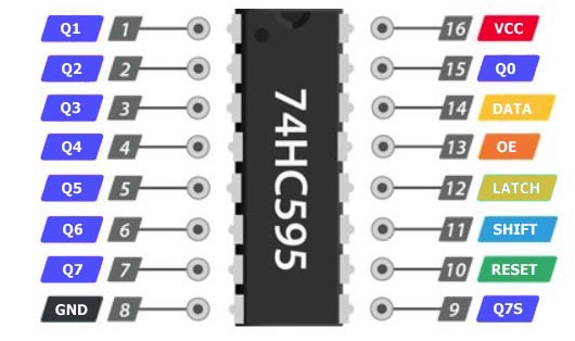
| PINS 7-15 | Q10-Q7 | Output Pins |
| PIN 8 | GND | Ground |
| PIN 9 | Q7S | Serial Out |
| PIN 10 | MR | RESET (Master Reclear, active low) |
| PIN 11 | SH_CP | SHIFT (Shift Register Clock Pin) |
| PIN 12 | ST_CP | LATCH (Storage Register Clock Pin) |
| PIN 13 | OE | Output Enable, active low |
| PIN 14 | DS | DATA (Serial data input) |
| PIN 16 | VCC | Positive Power Supply |
The 74HC595 is also a "Serial In Parallel Out" shift register. This means that you send your data in serial, so in short pulses to your chip. You send your input pulses to the DATA (DS) pin.
The pulses we send to our chip shift 1 place every time you pulse your SHIFT register clock pin (SH_CP). This means that if we give it a 1 as our first input pulse and then pulse our clock 7 times with a 0 as input we get 00000001.
10000000
01000000
00100000
00010000
00001000
00000100
00000010
00000001

Latched also means that our input is buffered before actually outputting, otherwise with a non-latched circuit you would visually see the 1 changing output pins. As long as the LATCH (ST_CP) pin is held low, we store our input data in the buffer, when we put the pin high the values in the buffer are latched to the storage register which are then outputted to the output pins (Q0 to Q7)
Another perk is the Master RESET (MR) pin. We can use this pin to clear all of our outputs and set everything to low.
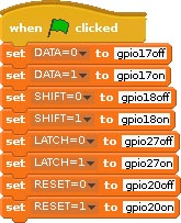 First we define variables for the GPIO pins we want to use. This is not necessary but it gives a better understanding of the script. We use variable names that correspond to its function. Then we specify for each variable the correct broadcast instruction to turn a GPIO pin on or off.
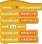 In the next step we perform a master reset to clear the register by setting the RESET pin to
 low and LATCH 00000000 to all output pins. Then we set the RESET pin to high. The RESET (MR) pin has to be always kept on high or the Shift Register won't function. The LATCH (ST_CP) pin has to set back to low to be ready for the next use.
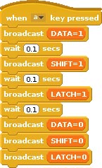 This script adds, shifts and latches another
 1 into the register each time you press the [A] botton. If you start from a cleared register after a RESET, then after 8 times pressing [A] you fill the register with 1's and one output pin after the other will be set on high.
00000000, 10000000, 11000000 ...... => 11111111
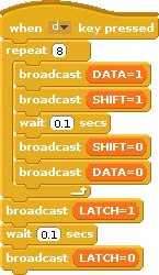 Here's a loop, that adds and shifts a
 1 automatically 8 times. After the register is filled with 1's, all of them are latched and all output pins will be set to high at once.
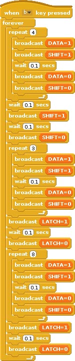 This script makes one output pin blink on and off while all other pins stay on. First 4
 1's are added and shifted into the register followed by a 0 and 3 more 1's which are then latched: => 11101111.
After this 8 1's are added, shifted and latched at once. All 8 output pins turn high. This script will loop forever creating a blink effect for pin Q3.
 You can use this script to stop the script above from running and to set the DATA, SHIFT and LATCH pins to
 0. After pressing [SPACE], press [R] to clear the register with the RESET script further up.